
LVDS (Low Voltage Differential Signaling) is a small amplitude differential signaling technology that uses very low amplitude signals (250mV~450mv) to transmit data through a pair of parallel PCB traces or balanced cables.
The current and voltage amplitudes flowing through the two parallel differential signal lines are opposite. The noise signal is coupled to the two lines at the same time. The receiving end only cares about the difference between the two signals, so the noise is canceled out. Since the electromagnetic fields around the two signal lines also cancel each other out, differential signal transmission has much smaller electromagnetic radiation than single-line signal transmission.
In addition, this transmission standard uses current mode drive output, which does not generate spike signals caused by ringing and signal switching, and has good EMI characteristics.
Because LVDS differential signaling technology reduces noise concerns, lower signal voltage amplitudes can be used. This feature is very important as it makes it possible to increase data transfer rates and reduce power consumption. Low drive amplitude means data can be inverted faster.
Since the driver is in constant current source mode, the power consumption hardly changes with frequency, and the power consumption of a single channel is very low.
Therefore, after using this technology, as long as the length of a pair of parallel transmission lines is consistent enough and good matching termination impedance technology is provided at the receiving end to reduce the generation of reflected signals, a very high data transmission rate can be provided.
Currently, it is very easy to provide a data transmission rate of 840MHZ without complicated and special processing.
2
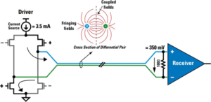
LVDS driver and receiver
The above figure is a schematic diagram of the working principle of LVDS. Its driver consists of a constant current source (usually 3.5mA) driving a pair of differential signal lines. There is a high DC input impedance at the receiver (nearly no current drawn), so almost all of the drive current will flow through the 100 ohm termination resistor producing a voltage of about 350mV at the receiver input.
When the drive state is reversed, the direction of the current flowing through the resistor changes, thus producing a valid “0” or “1” logic state at the receiving end. LVDS technology features include:
1. High-speed transmission capability, the transmission capability of LVDS can reach up to 2Gbps;
2. Low voltage and low power consumption. LVDS is implemented using CMOS technology and has low static power consumption;
3. Low noise radiation;
4. Using differential transmission mode has strong anti-interference ability;
LVDS has many advantages over traditional single-ended signal topologies (such as parallel LVTTL/LVCNOS). The main advantages include EMI (electromagnetic interference) reduction, faster data rates, longer extended transmission distances, and cost and convenience.
3
For Gen 2 and Gen 3 LVDS SerDes (serializer/deserializer), another benefit is increased system reliability and reduced EMI through RBS (randomization, DC balancing, scrambling) encoding. A static display image can contain many identical color bits, which can produce DC drift and affect signal quality as well as create EMI spikes. RBS encoding randomizes the data and scrambles the bit positions, removing static patterns and ensuring correct conversions, then balancing the DC to allow AC coupling and provide isolation. The end result of this encoding is less jitter and spread over more of the transmission spectrum to reduce EMI.
Data rate, distance and cost/convenience
Data rate is another benefit of LVDS over LVTTL/LVCMOS since the data rate of the parallel interface is very limited. As mentioned earlier, when many outputs are transmitted in parallel, the faster each signal travels, the more EMI it generates. In addition, inter-signal delay differences also limit the distance a signal can travel, which gets worse at faster data rates. With LVDS, data rates can be higher and distances can be extended to more than 10 meters. PCB design is also much easier as length matching considerations are reduced and more space is available.
4
During the design process, consider the following:
• EMI
LVDS signal filtering design is mainly designed for clock signals and bus signals. The clock signal adds an RC filter design at the transmitting end to reduce the external radiation interference of the clock. For differential signals, the filtering design requires adding a common mode inductor at the port for filtering. Common mode noise suppression.
The anti-interference design of LVDS signals is divided into fixed path interference and environmental interference.
• Fixed path interference
The interference path is usually the power supply or signal line, so the LVDS circuit design only needs to add a protective design to the interface. The interface adds magnetic beads to absorb and then adds capacitance to the ground, so that the interference can be discharged through the fastest path.
• Environmental interference
This interference is caused by electromagnetic radiation from external sources in the environment, and protection measures such as the addition of ferrite beads and capacitors are often used to reduce the effects of this interference.
• To reduce crosstalk between single-ended signals and LVDS signals, you should follow:
1. On the same PCB layer, the single-ended signal should be at least 12 mm away from the LVDS signal;
2. The distance between differential lines should not exceed twice the width of the signal lines, and the thickness of the circuit board should be greater than the distance between signal lines;
3. The distance between two adjacent differential pairs should be greater than or equal to 2 times the distance between independent signal lines.
• Impedance matching
When designing impedance matching for LVDS signals, you should follow:
1. The PCB should be at least a 4-layer board. LVDS signals and TTL/CMOS signals need to be isolated by a power layer or ground layer; the LVDS driver and receiver should be placed as close to the connector as possible;
2. Place a 4.7μF or 10μF capacitor close to the Vcc pin of the driver or receiver, and consider the matching of the working frequency of the signal and the best working frequency of the capacitor;
3. Place at least one 0.1μF and one 0.001μF capacitor close to a driver or receiver Vcc pin;
4. Make the power supply and ground wires as wide as possible to reduce the power return impedance.
Learn More:What is the function of LVDS?